2. I/O Interface
The VIA EPIA-P910 has a wide selection of interfaces. It includes a selection of frequently used ports as part of the external I/O coastline.
2.1. External I/O Ports

Figure 1: External I/O ports
Layout diagram description table of external I/O ports:
| Item | Description |
|---|---|
| 1 | RJ1: Gigabit LAN port |
| 2 | USB1: USB 3.0 ports |
| 3 | USB2: USB 3.0 ports |
| 4 | HDMI1: Mini HDMI® port |
| 5 | VGA1: VGA port |
2.1.1. LAN port: Gigabit Ethernet
The integrated 8-pin Gigabit Ethernet port is using an 8 Position 8 Contact (8P8C) receptacle connector (commonly referred to as RJ45). The Gigabit Ethernet ports are controlled by VIA Fast Ethernet controller. The pinout of the Gigabit Ethernet port is shown below:

Figure 2: Gigabit Ethernet port pinout diagram
Gigabit Ethernet port pinout:
| Pin | Signal |
|---|---|
| 1 | Signal pair 1+ |
| 2 | Signal pair 1- |
| 3 | Signal pair 2+ |
| 4 | Signal pair 3+ |
| 5 | Signal pair 3- |
| 6 | Signal pair 2- |
| 7 | Signal pair 4+ |
| 8 | Signal pair 4- |
The RJ-45 port has two individual LED indicators located on the front side to show its Active/Link status and Speed status.
Gigabit Ethernet LED color definition:
| State | Link LED (Left LED) | Active LED (Right LED) |
|---|---|---|
| Link Off | Off | Off |
| Speed 10Mbit | The LED is always On in either Green or Orange colors | Flash in Yellow color |
| Speed 100Mbit | The LED is always On in Green color | Flash in Yellow color |
| Speed 1000Mbit | The LED is always On in Orange color | Flash in Yellow color |
2.1.2. USB 3.0 Port
The EPIA-P910 mainboard provides two USB 3.0 ports, also known as SuperSpeed USB. The USB 3.0 port has a maximum data transfer rate up to 5 Gbps and offers a backwards compatible with previous USB 2.0 specifications. The USB 3.0 ports are using the USB Type-A receptacle connector. The pinout of the typical USB 3.0 port is shown below.

Figure 3: USB 3 .0 port pinout diagram
USB 3.0 port pinout:
| Pin | Signal |
|---|---|
| 1 | +5V |
| 2 | Data- |
| 3 | Data+ |
| 4 | GND |
| 5 | Rx- |
| 6 | Rx+ |
| 7 | GND |
| 8 | Tx- |
| 9 | Tx+ |
2.1.3. Mini HDMI Port
The integrated 19-pin HDMI® port uses an HDMI® Type C connector as defined in the HDMI® specification. The HDMI® port is for connecting to HDMI® displays. The pinout of the Mini HDMI® port is shown below.
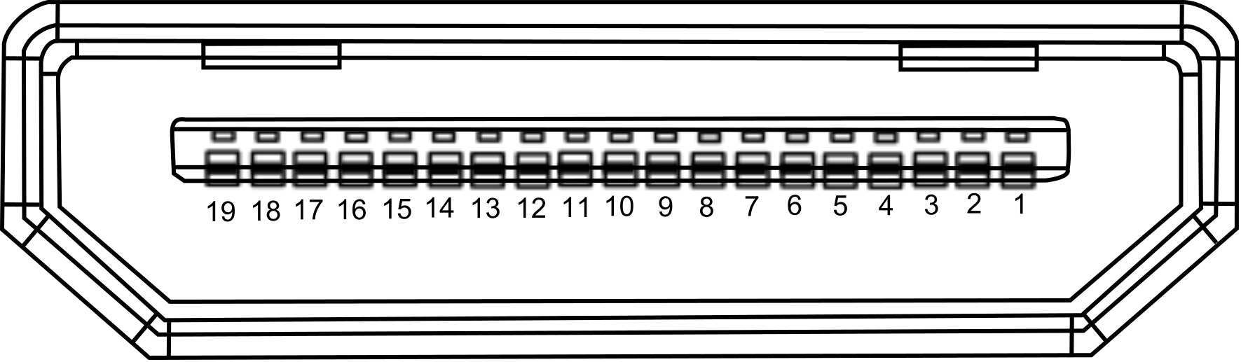
Figure 4: Mini HDMI® port pinout diagram
| Pin | Signal | Pin | Signal |
|---|---|---|---|
| 1 | TMDS Data2 Shield | 2 | TMDS Data2+ |
| 3 | TMDS Data2- | 4 | TMDS Data1 Shield |
| 5 | TMDS Data1+ | 6 | TMDS Data1– |
| 7 | TMDS Data0 Shield | 8 | TMDS Data0+ |
| 9 | TMDS Data0- | 10 | TMDS Clock Shield |
| 11 | TMDS Clock+ | 12 | TMDS Clock- |
| 13 | DDC/CEC Ground | 14 | CEC |
| 15 | SCL | 16 | SDA |
| 17 | Reserved (N.C. on device) | 18 | +5V Power |
| 19 | Hot Plug Detect |
2.1.4. VGA Port
The 15-pin VGA port uses a female DE-15 connector. The VGA port is for connecting to analog displays. The pinout of the VGA port is shown below.

Figure 5: VGA port pinout diagram
VGA port pinout:
| Pin | Signal | Pin | Signal |
|---|---|---|---|
| 1 | VGA-R | 9 | +5VCRT |
| 2 | VGA-G | 10 | Ground |
| 3 | VGA-B | 11 | NC |
| 4 | NC | 12 | VGA-SPD |
| 5 | Ground | 13 | VGA_HS |
| 6 | Ground | 14 | VGA_VS |
| 7 | Ground | 15 | VGA-SPCLK |
| 8 | Ground |
2.2. Onboard Connectors
2.2.1. LVDS Connector
The mainboard has one 24-pin LVDS panel connector on the bottom side. The onboard LVDS panel connector allows to connect the panel’s LVDS cable to support the single-channel 18-bit/24-bit display. Backlight controls are integrated into the LVDS panel connector pinout. The LVDS panel connector is labeled as “LVDS1”. The pinout of the connector is shown below.
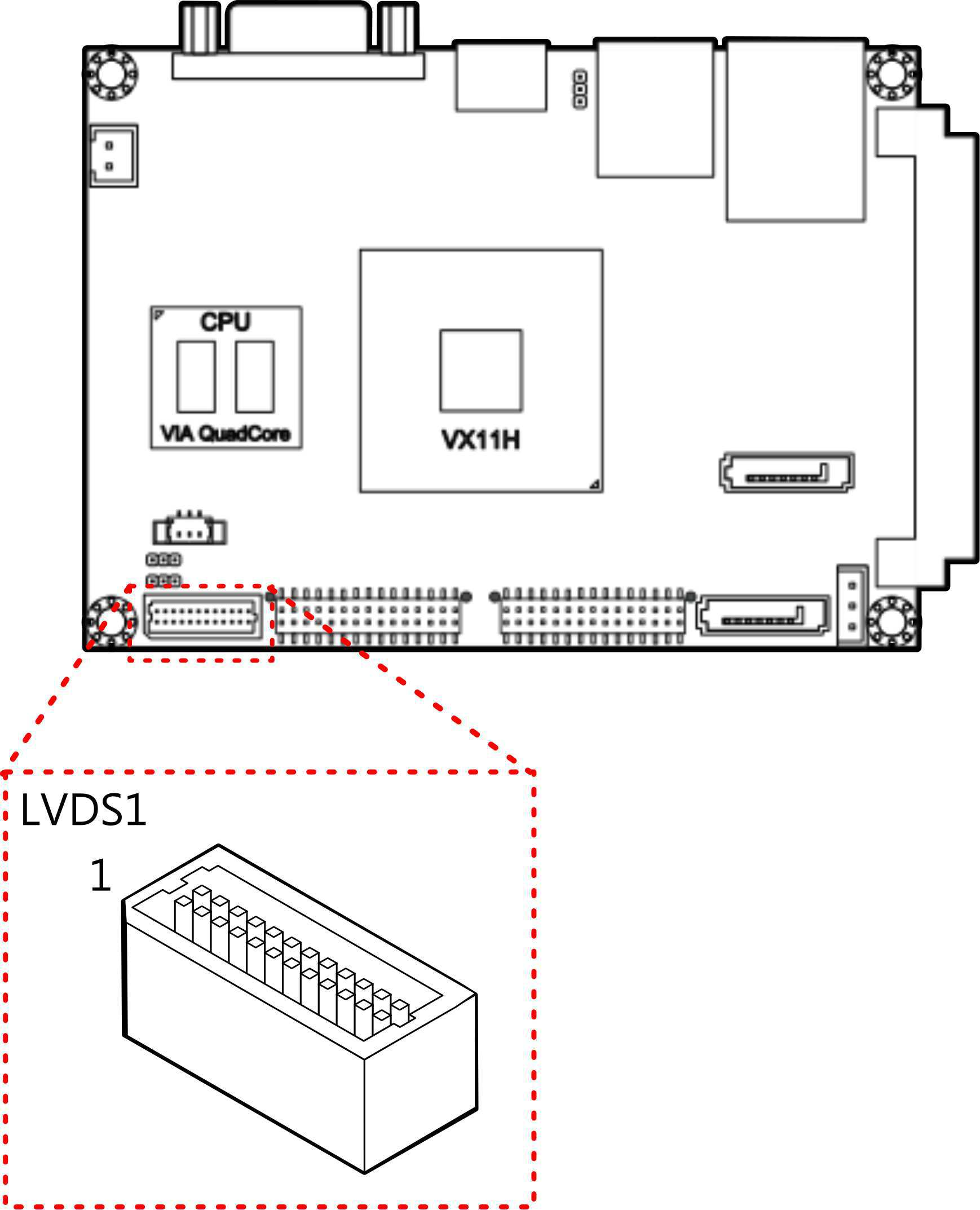
Figure 6: LVDS connector
LVDS connector pinout:
| Pin | Signal | Pin | Signal |
|---|---|---|---|
| 1 | LVDSD0- | 2 | LVDSD1- |
| 3 | LVDSD0+ | 4 | LVDSD1+ |
| 5 | GND | 6 | GND |
| 7 | PVDD2 | 8 | LVDSD2- |
| 9 | PVDD2 | 10 | LVDSD2+ |
| 11 | LCD1_DATA | 12 | GND |
| 13 | LCD1_CLK | 14 | LVDSCLK+ |
| 15 | GND | 16 | LVDSCLK- |
| 17 | VDD_BL | 18 | GND |
| 19 | VDD_BL | 20 | LVDSD3- |
| 21 | BLEN_1 | 22 | LVDSD3+ |
| 23 | BAK_ADJ | 24 | GND |
Note
LVDS1 supports 18/24 bits EDID LCD, please ensure your LCD do support EDID. For any request of None-EDID LCD, please contact sales for customized BIOS support
2.2.2. SATA Connectors
The two SATA connectors onboard can support up to 3 Gb/s transfer speeds. Both SATA connectors have a 7th pin 1 that can provide +5V power to a SATA Disk-on-Module (DOM). When a regular SATA hard drive is connected, the 7th pin will be a ground pin. The SATA connectors are labeled as “SATA1” and “SATA2”. The pinout of the SATA connectors are shown below.
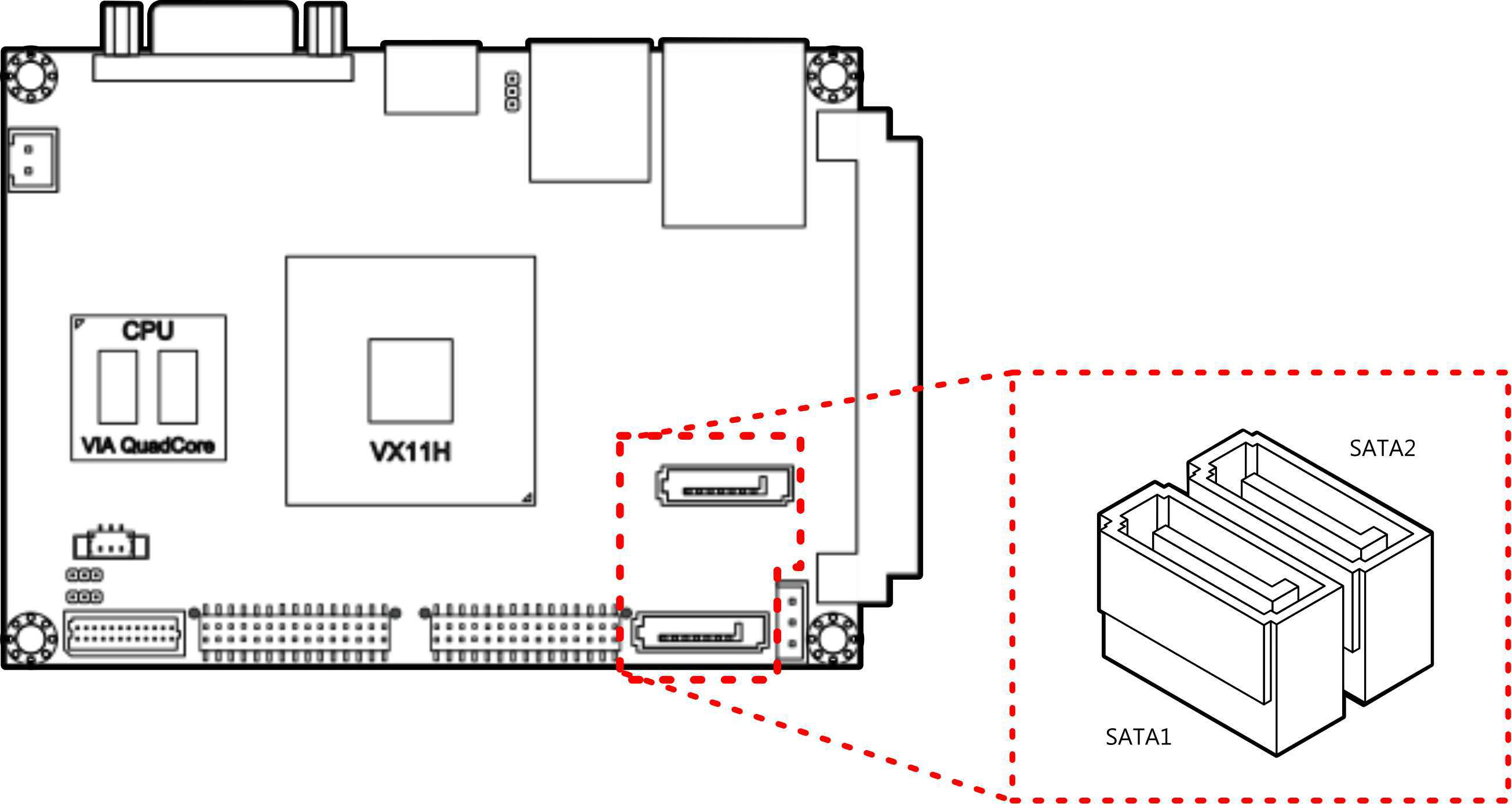
Figure 7: SATA connectors
SATA connector pinouts:
| SATA1 Pin | Signal | SATA2 Pin | Signal |
|---|---|---|---|
| 1 | GND | 1 | GND |
| 2 | STXP_0 | 2 | STXP_1 |
| 3 | STXN_0 | 3 | STXN_1 |
| 4 | GND | 4 | GND |
| 5 | SRXN_0 | 5 | SRXN_1 |
| 6 | SRXP_0 | 6 | SRXP_1 |
| 7 | GND/+5V | 7 | GND/+5V |
Note
The SATA connector pin 7 default setting is GND. The +5V supports is a factory option.
2.2.3. SATA Power Connector
The onboard SATA power connector provides both +5V and +12V directly through the mainboard to the SATA drives. The SATA power connector is labeled as “PWR2”. The pinout of the SATA power connector is shown below.
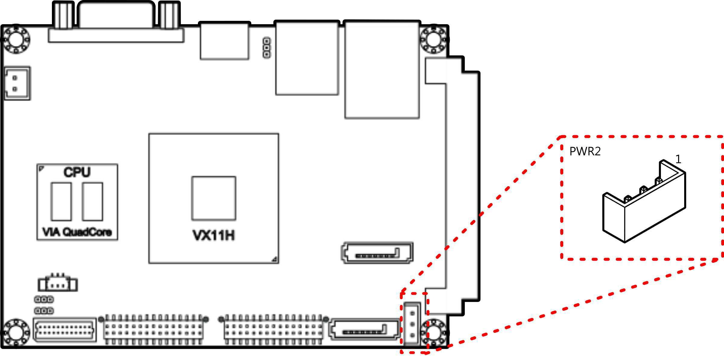
Figure 8: SATA power connector
SATA power connector pinout:
| Pin | Signal |
|---|---|
| 1 | +5V/1A |
| 2 | +12V/1A |
| 3 | GND |
2.2.4. KB/MS/LPC/GPIO/SMBus Combination Pin Header
The mainboard includes one KB, MS, LPC, GPIO and SMBus combination pin header block labeled as “CN1”. The combination pin header is for connecting KB, MS, LPC, General Purpose Input and Output and SMBus devices. The pinout of the pin header is shown below.
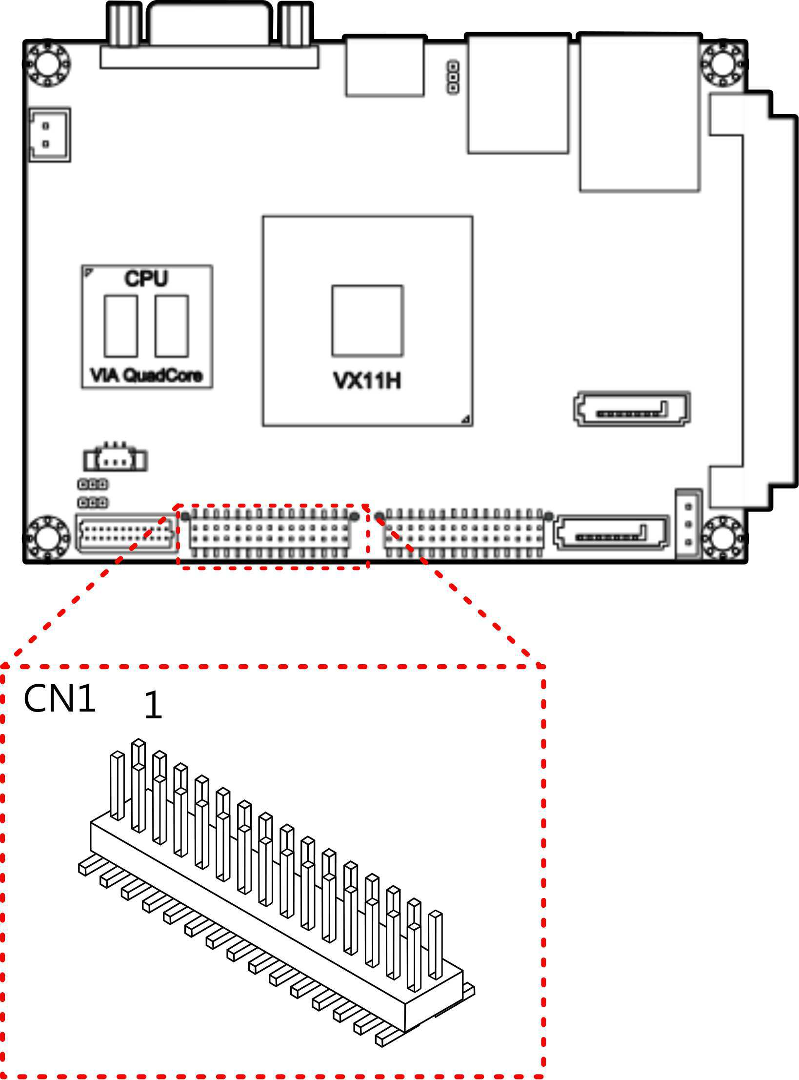
Figure 9: KB/MS/LPC/GPIO/ SMBus combination pin header
KB/MS/LPC/GPIO/SMBus combination pin header pinout:
| Pin | Signal | Pin | Signal |
|---|---|---|---|
| 1 | LAD3 | 2 | GND |
| 3 | LAD2 | 4 | SIO_CLK1 |
| 5 | LAD1 | 6 | PCICLK3 |
| 7 | -LFRAME | 8 | -LDRQ0 |
| 9 | LAD0 | 10 | SERIRQ |
| 11 | -PCIRST | 12 | GND |
| 13 | SMBDT_+3.3V | 14 | SMBCK_+3.3V |
| 15 | +3.3V | 16 | +5V |
| 17 | -LID/GPI7 | 18 | -INTB/GPIO8 |
| 19 | -THRM/GPI9 | 20 | -INTC/GPIO9 |
| 21 | -EXTSMI/GPI5 | 22 | GPIO12/GPIO12 |
| 23 | -BATLOW/GPI4 | 24 | GPIO32/GPIO32 |
| 25 | GND | 26 | +5VSUS |
| 27 | KBDT | 28 | KBCK |
| 29 | MSDT | 30 | MSC |
2.2.5. Audio + USB 2.0 + Front Panel Combination Pin Header
The mainboard includes one USB 2.0, Front Panel and Audio combination pin header block labeled as “CN2”.The USB 2.0, front panel and audio combination pin header is used to enable up to three USB 2.0 ports and to connect the power switch, reset switch, power LED, suspend LED, HDD LED, case speaker, SPDIF out, Line-Out, Line-In and MIC-In jacks. The pinout of the pin header is shown below.
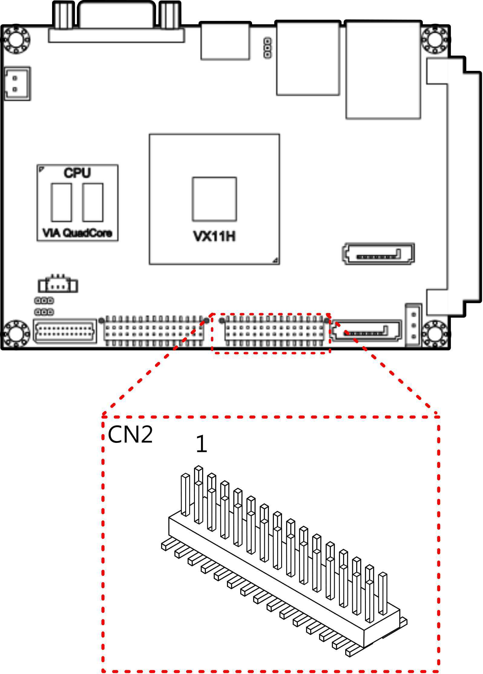
Figure 10: Audio + USB + Front panel combination pin header
Audio + USB + Front panel combination pin header pinout:
| Pin | Signal | Pin | Signal |
|---|---|---|---|
| 1 | GND | 2 | +5VSUSH1 |
| 3 | USB_VD0- | 4 | USB_VD0+ |
| 5 | USB_VD1- | 6 | USB_VD1+ |
| 7 | USB_VD5- | 8 | USB_VD5+ |
| 9 | GND | 10 | GND |
| 11 | +5V | 12 | +5VSUS |
| 13 | -HD_LED | 14 | -PWR_LED |
| 15 | PW_BN1- | 16 | GND |
| 17 | GND | 18 | SPEAK_BZ |
| 19 | RST_SW | 20 | GND |
| 21 | GND_AUD | 22 | LINER |
| 23 | MICIN_L | 24 | LINEL |
| 25 | MICIN_R | 26 | LINEOUT_R |
| 27 | SENSE_A | 28 | LINEOUT_L |
| 29 | SPDIF_TX0 | 30 | GND |
2.2.6. System/CPU Fan Connector
The System/CPU fan connector onboard runs on +12V and maintain system/CPU cooling. The fan provides variable fan speeds controlled by the BIOS. The System/CPU fan connector is labeled as “FAN1”. The pinout of the system/fan connector is shown below.
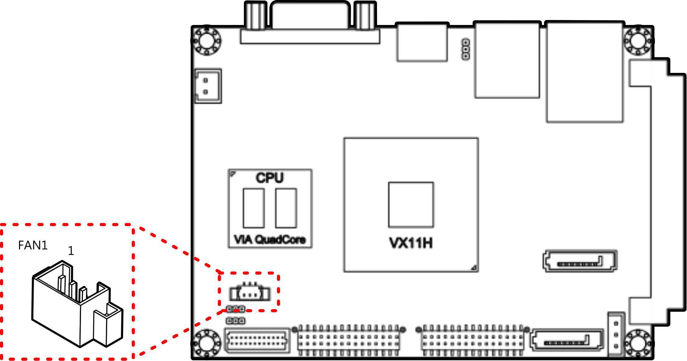
Figure 11: System/CPU fan connector
System/CPU fan an connector pinout:
| Pin | Signal |
|---|---|
| 1 | FANIN1 |
| 2 | +12V FAN |
| 3 | GND |
2.2.7. DC-In Power Connector
The mainboard has an onboard DC-In 2-pin power connector to connect the DC-In power cable. The DC-In power connector is labeled as “PWR1”. The pinout of the DC-In power connector is shown below.
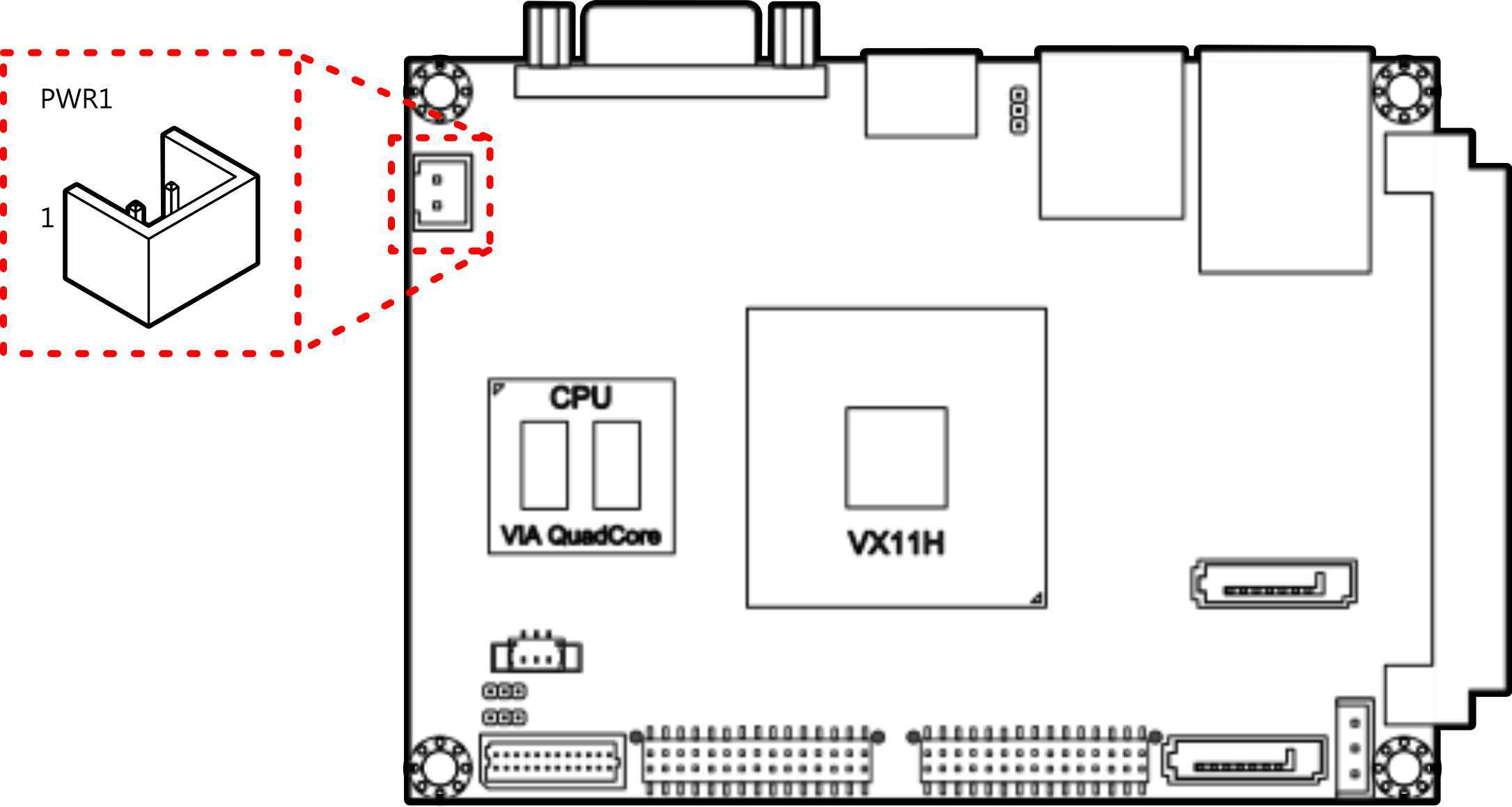
Figure 12: DC-In power connector
DC-In power connector pinout:
| Pin | Signal |
|---|---|
| 1 | +12V |
| 2 | GND |
2.2.8. CMOS Battery Connector
The mainboard is equipped with onboard CMOS battery connector used for connecting the external cable battery that provides power to the CMOS RAM. If disconnected all configurations in the CMOS RAM will be reset to factory defaults. The CMOS battery connector is labeled as “BAT1”. The connector pinout is shown below.
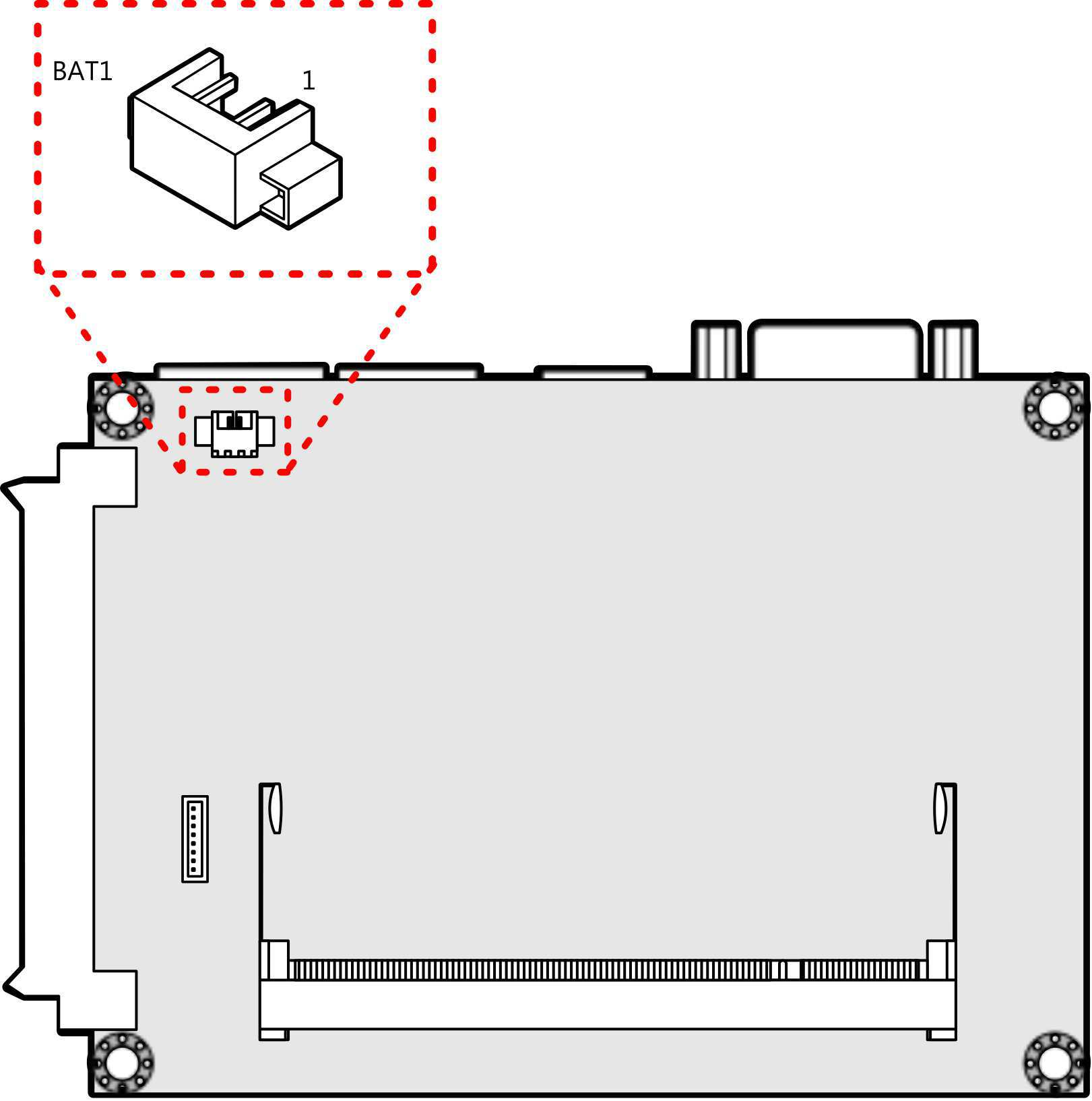
Figure 13: CMOS battery connector
CMOS battery connector pinout:
| Pin | Signal |
|---|---|
| 1 | RTC_BAT |
| 2 | GND |
2.2.9. SPI Flash Connector
The mainboard has one 8-pin SPI flash connector. The SPI (Serial Peripheral Interface) flash connector is used to connect to the SPI BIOS programming fixture for updating the SPI flash ROM. The connector is labeled as “J1”. The pinout of the connector is shown below.
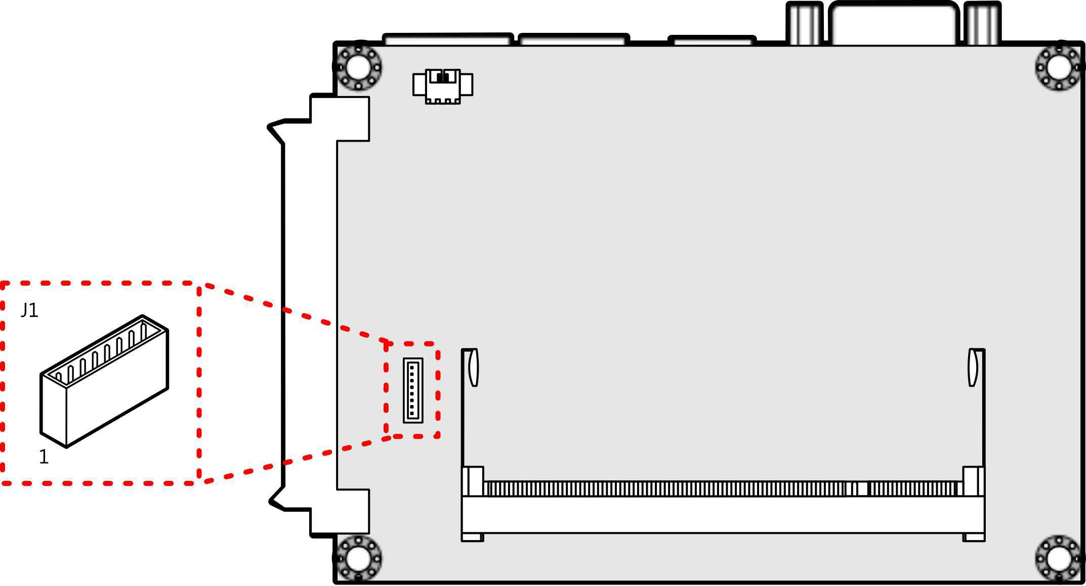
Figure 14: SPI connector
SPI connector pinout:
| Pin | Signal |
|---|---|
| 1 | NC |
| 2 | NC |
| 3 | MSPIDO |
| 4 | MSPIDI |
| 5 | MSPICLK |
| 6 | MSPISSO |
| 7 | GND |
| 8 | SPIVCC |