2. I/O Interface
The VAB-820 has a wide selection of interfaces. It includes a selection of frequently used ports as part of the external I/O coastline.
2.1. External I/O Ports

Figure 1: Rear I/O ports

Figure 2: Front I/O ports
Layout diagram description table of rear I/O ports:
| Item | Description |
|---|---|
| 1 | J16: RJ-45 LAN port |
| 2 | USB1: USB 2.0 port 2 |
| 3 | USB0: USB 2.0 port 1 |
| 4 | HDMI1: HDMI® port |
| 5 | J15 : Composite input RCA jack |
| 6 | Micro SD card slot |
2.1.1. RJ-45 LAN port: Gigabit Ethernet
The integrated 8-pin Gigabit Ethernet port is using an 8 Position 8 Contact (8P8C) receptacle connector (commonly referred to as RJ45). The pinout of the Gigabit Ethernet port is shown below.

Figure 3: Gigabit Ethernet port pinout diagram
Gigabit Ethernet port pinout:
| Pin | Signal |
|---|---|
| 1 | Signal pair 1+ |
| 2 | Signal pair 1- |
| 3 | Signal pair 2+ |
| 4 | Signal pair 3+ |
| 5 | Signal pair 3- |
| 6 | Signal pair 2- |
| 7 | Signal pair 4+ |
| 8 | Signal pair 4- |
The Gigabit Ethernet port (RJ45 port) has two individual LED indicators located on the front side to show its Active/Link status and Speed status.
Gigabit Ethernet LED color definition:
| Connection | Link LED (Left LED on RJ-45 connector) | Active LED (Right LED on RJ-45 connector) |
|---|---|---|
| Link Off | Off | Off |
| Speed_10Mbit | The LED is always On in Orange color | Flash in Yellow color |
| Speed_100Mbit | The LED is always On in Orange color | Flash in Yellow color |
| Speed_1000Mbit | The LED is always On in Orange color | Flash in Yellow color |
2.1.2. USB 2.0 Port
The VAB-820 mainboard provides two USB 2.0 ports, each USB port gives complete Plug and Play and hot swap capability for external devices. The USB interface complies with USB UHCI, Rev. 2.0. The pinout of the typical USB 2.0 port is shown below.

Figure 4: USB 2.0 port diagram
USB 2.0 port pinout:
| USB1 | USB2 | ||
|---|---|---|---|
| Pin | Signal | Pin | Signal |
| 1 | VCC | 1 | VCC |
| 2 | USB data - | 2 | USB data - |
| 3 | USB data + | 3 | USB data + |
| 4 | GND | 4 | GND |
2.1.3. HDMI® Port
The integrated 19-pin HDMI® port uses an HDMI® Type A receptacle connector defined in HDMI specification. The HDMI® port is used to connect high definition video and digital audio using a single cable. It allows connecting the digital video devices which utilize a high definition video signal. The pinout of the HDMI® port is shown below.

Figure 5: HDMI® port diagram
HDMI® port pinout:
| Pin | Signal | Pin | Signal |
|---|---|---|---|
| 1 | TMDS Data0+ | 2 | GND |
| 3 | TMDS Data0– | 4 | TMDS Data1+ |
| 5 | GND | 6 | TMDS Data1– |
| 7 | TMDS Data2+ | 8 | GND |
| 9 | TMDS Data2– | 10 | TMDS Data3+ |
| 11 | GND | 12 | TMDS Data3– |
| 13 | CEC | 14 | NC |
| 15 | HDMI Clock | 16 | HDMI Data |
| 17 | GND | 18 | HDMI Power |
| 19 | Hot Plug Detect |
2.1.4. RCA Jack
The RCA jack connects to external composite video input device.
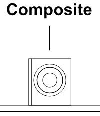
Figure 6: RCA jack diagram
RCA Jack pinout:
| Description | RCA Jack |
|---|---|
| Video Composite | Video Input |
2.1.5. Micro SD Card slot
There is a Micro SD card slot located on the front I/O panel. The Micro SD card slot offers expandable storage.

Figure 7: Micro SD card slot diagram
Micro SD card slot pinout:
| Pin | Signal |
|---|---|
| 1 | SD0DATA2 |
| 2 | SD0DATA3 |
| 3 | SD0CMD |
| 4 | VDD (3.3V) |
| 5 | SD0CLK |
| 6 | GND |
| 7 | SD0DATA0 |
| 8 | SD0DATA1 |
| 9 | SD0_CD |
2.2. Onboard Connectors
2.2.1. USB, USBOTG Pin Header
The mainboard includes one USB and USBOTG combination pin header block labeled as “J8”. The combination pin header is used for connecting USB and USBOTG devices. The pinout of the pin header is shown below.

Figure 8: USB, USBOTG pin header diagram
USB, USBOTG pin header pinout:
| Pin | Signal | Pin | Signal |
|---|---|---|---|
| 1 | GND | 2 | – |
| 3 | USB_OTG_ID | 4 | GND |
| 5 | OTG_DP | 6 | USBD_T3+ |
| 7 | OTG_DN | 8 | USBD_T3- |
| 9 | OTG_VBUS | 10 | USB_VBUS |
2.2.2. Front Audio Pin Header
The mainboard has a pin header for Line-out, Line-in and MIC-in. This pin header is labeled as “AUDIO1”. The pinout of the pin header is shown below.

Figure 9: Front Audio pin header diagram
Front Audio pin header pinout:
| Pin | Signal | Pin | Signal |
|---|---|---|---|
| 1 | HEAD_RIGHT | 2 | HEAD_LEFT |
| 3 | LINE_IN_R | 4 | LINE_IN_L |
| 5 | MIC_IN | 6 | MIC_IN |
| 7 | – | 8 | NC |
| 9 | GND_ANALOG | 10 | GND_ANALOG |
2.2.3. DIO, I²C, System reset, P_LED, and WLAN_LED Pin Header
The mainboard includes one DIO, I²C, System reset, P_LED, and WLAN_LED combination pin header block labeled as “J7”. The combination pin header is used for connecting Digital I/O (GPIO), I²C devices and providing access to system reset switch, power LED and WLAN LED. The pinout of the pin header is shown below.

Figure 10: DIO, I²C, System reset, P_LED, and WLAN_LED combination pin header diagram
DIO, I²C, System reset, P_LED, and WLAN_LED pin header pinout:
| Pin | Signal | Pin | Signal |
|---|---|---|---|
| 1 | RESET_N | 2 | P_LED+ |
| 3 | GND | 4 | P_LED- |
| 5 | I2C3_SCL | 6 | W_LED+ |
| 7 | I2C3_SDA | 8 | W_LED- |
| 9 | 5VIN | 10 | GND |
| 11 | GPIO_1 | 12 | GPIO_7 |
| 13 | GPIO_2 | 14 | GPIO_8 |
| 15 | GPIO_4 | 16 | GPIO_9 |
| 17 | GPIO_5 | 18 | GPIO_16 |
| 19 | GND | 20 | – |
2.2.4. SPI connector
The mainboard has one 7-pin SPI flash connector. The SPI (Serial Peripheral Interface) connector is used to communicate with external slave devices. The connector is labeled as “J10”. The pinout of the connector is shown below.

Figure 11: SPI connector diagram
SPI connector pinout:
| Pin | Signal |
|---|---|
| 1 | CSPI3_CLK |
| 2 | CSPI3_MOSI |
| 3 | CSPI3_MISO |
| 4 | 3P3V |
| 5 | CSPI3_CS0 |
| 6 | GND |
| 7 | CSPI3_CS1 |
2.2.5. PoE Pin Header
The mainboard has two PoE pin headers. The PoE pin headers are used to connect to optional PD power board for implementation of Power Over Ethernet. The PoE input connector is labeled as “J13”. The PoE output connector is labeled as “J14”. The pinout of the connector is shown below.

Figure 12: PoE Output/Input pin header diagram
PoE Output pin (J14) header pinout:
| Pin | Signal | Pin | Signal |
|---|---|---|---|
| 1 | POE_12V | 2 | POE_12V |
| 3 | NC | 4 | – |
| 5 | GND | 6 | GND |
PoE Input pin (J13) header pinout:
| Pin | Signal | Pin | Signal |
|---|---|---|---|
| 1 | WIRE1 | 2 | WIRE2 |
| 3 | NC | 4 | – |
| 5 | WIRE3 | 6 | WIRE4 |
2.2.6. +12V DC-In Connector
The mainboard has a +12V DC-In power connector to provide additional power to the rest of the system. The 2-pin power connector is used to connect the DC-In power jack. The connector is labeled as “J9”. The pinout of the connector is shown below.

Figure 13: 12V DC-In connector diagram
12V DC-In connector pinout:
| Pin | Signal |
|---|---|
| 1 | +12V |
| 2 | GND |
2.2.7. S-Video Input Pin Header
The mainboard provides an S-Video Input pin header. The S-Video Input pin header is an analog video connector for connecting TV monitor or S-Video input devices. The pinout of the S-Video input pin header is shown below.

Figure 14: S-Video input pin header diagram
S-Video input pin header pinout:
| Pin | Signal | Pin | Signal |
|---|---|---|---|
| 1 | C | 2 | GND |
| 3 | Y | 4 | – |
| 5 | NC | 6 | GND |
2.2.8. CMOS Battery Connector
The mainboard is equipped with an onboard CMOS battery connector used for connecting the external cable battery that provides power to the CMOS RAM. If disconnected all configurations in the CMOS RAM will be reset to factory defaults. The CMOS battery connector is labeled as “J1”. The connector pinout is shown below.

Figure 15: CMOS battery connector diagram
CMOS battery connector pinout:
| Pin | Signal |
|---|---|
| 1 | +VBAT |
| 2 | GND |
2.2.9. Mini-PCIe Slot
The Mini-PCIe slot is compatible with all PCIe 2.0 Mini Cards: full-length and half-length. The location of the Mini-PCIe slot is shown below.

Figure 16: Mini-PCIe slot diagram
Mini-PCIe slot pinout:
| Pin | Signal | Pin | Signal |
|---|---|---|---|
| 1 | PCIE_WAKE_B | 2 | MPCIE_3V3 |
| 3 | GND | 4 | GND |
| 5 | JTAG_TCK | 6 | VCC15 |
| 7 | JTAG_TMS | 8 | – |
| 9 | GND | 10 | NC |
| 11 | PCIe_CREFCLKM | 12 | NC |
| 13 | PCIe_CREFCLKP | 14 | NC |
| 15 | GND | 16 | – |
| 17 | JTAG_TD1 | 18 | GND |
| 19 | JTAG_TD0 | 20 | PCIE_DIS_B |
| 21 | GND | 22 | PCIE_RST_B |
| 23 | PCIe_CRXM | 24 | MPCIE_3V3 |
| 25 | PCIe_CRXP | 26 | GND |
| 27 | GND | 28 | VCC15 |
| 29 | GND | 30 | PCIe_SMB_CLK |
| 31 | PCIe_CTXM | 32 | PCIe_SMB_DATA |
| 33 | PCIe_CTXP | 34 | GND |
| 35 | GND | 36 | PCIE_USB_DM |
| 37 | GND | 38 | PCIE_USB_DP |
| 39 | MPCIE_3V3 | 40 | GND |
| 41 | MPCIE_3V3 | 42 | LED_WWAN_B |
| 43 | GND | 44 | LED_WLAN_B |
| 45 | JTAG_nTRST | 46 | LED_WPAN_B |
| 47 | JTAG_nSRST | 48 | VCC15 |
| 49 | GND | 50 | GND |
| 51 | NC | 52 | MPCIE_3V3 |
2.2.10. LVDS1 Connector
The mainboard has one 40-pin LVDS panel connector on the bottom side. The onboard LVDS panel connector allows to connect the panel’s LVDS cable to support the dual-channel 18-bit/24-bit display. Backlight controls are integrated into the LVDS panel connector pinout. The LVDS panel connector is labeled as “LVDS1”. The pinout of the connector is shown below.

Figure 17: LVDS1 connector diagram
LVDS1 connector pinout:
| Pin | Signal | Pin | Signal |
|---|---|---|---|
| 1 | LVDS1_TX0_NC | 2 | PVDD |
| 3 | LVDS1_TX0_PC | 4 | PVDD |
| 5 | GND | 6 | GND |
| 7 | LVDS1_TX1_NC | 8 | GND |
| 9 | LVDS1_TX1_PC | 10 | LVDS0_TX0_NC |
| 11 | GND | 12 | LVDS0_TX0_PC |
| 13 | LVDS1_TX2_NC | 14 | GND |
| 15 | LVDS1_TX2_PC | 16 | LVDS0_TX1_NC |
| 17 | GND | 18 | LVDS0_TX1_PC |
| 19 | LVDS1_CLK_NC | 20 | GND |
| 21 | LVDS1_CLK_PC | 22 | LVDS0_TX2_NC |
| 23 | GND | 24 | LVDS0_TX2_PC |
| 25 | LVDS1_TX3_NC | 26 | GND |
| 27 | LVDS1_TX3_PC | 28 | LVDS0_CLK_NC |
| 29 | GND | 30 | LVDS0_CLK_PC |
| 31 | 5VIN | 32 | GND |
| 33 | 3P3V | 34 | LVDS0_TX3_NC |
| 35 | NC | 36 | LVDS0_TX3_PC |
| 37 | NC | 38 | LVDS0_EDID_SCL |
| 39 | NC | 40 | LVDS0_EDID_SDA |
2.2.11. LVDS Inverter Connector
The mainboard has one LVDS Inverter connector located on the bottom side of the board for supplying power to the backlight of the LCD panel. The connector is labeled as “INVERTER”. The pinout of the connector is shown below.

Figure 18: LVDS Inverter Connector diagram
LVDS Inverter Connector pinout:
| Pin | Signal |
|---|---|
| 1 | IVDD |
| 2 | IVDD |
| 3 | LVDS_EN |
| 4 | DISP0_CONTRAST |
| 5 | LVDS_EN |
| 6 | DISP0_CONTRAST |
| 7 | GND |
| 8 | GND |
2.2.12. MIPI CSI-2 Connector
The mainboard includes one MIPI CSI-2 connector on the bottom side of the board. The MIPI CSI-2 connector is used to connect to a camera serial interface in order to support a wide range of imaging solutions. The connector is labeled as “J18”. The pinout of the connector is shown below.

Figure 19: MIPI CSI-2 connector diagram
MIPI CSI-2 connector pinout:
| Pin | Signal |
|---|---|
| 1 | 5VIN |
| 2 | I2C2_SCL |
| 3 | I2C2_SDA |
| 4 | GND |
| 5 | CSI_CLK0P |
| 6 | CSI_CLK0M |
| 7 | GND |
| 8 | CSI_D0P |
| 9 | CSI_D0M |
| 10 | GND |
| 11 | CSI_D1M |
| 12 | CSI_D1P |
2.2.13. COM1/COM2/CAN Connector
The mainboard includes two onboard COM connectors on the bottom side of the board. The onboard COM1 connector labeled as “J4” is used to attach additional COM ports that support RS-232 standard with DTE (Data Terminal Equipment) type. The onboard COM2/CAN connector labeled as “J5” is primarily used to attach additional COM port for debug purpose. The CAN bus can also be supported through this connector. The pinout of the connector is shown below.

Figure 20: COM1/COM2/CAN connector diagram
COM1/COM2/CAN connector pinout:
| COM1 | COM2/CAN | ||
|---|---|---|---|
| Pin | Signal | Pin | Signal |
| 1 | 5VIN | 1 | 5VIN |
| 2 | COM_RXD1 | 2 | COM2_RX |
| 3 | COM_TXD1 | 3 | COM2_TX |
| 4 | COM_DCD1 | 4 | NC |
| 5 | COM_RI1 | 5 | NC |
| 6 | GND | 6 | GND |
| 7 | COM_DTR1 | 7 | CAN_RX2 |
| 8 | COM_CTS1 | 8 | CAN_TX2 |
| 9 | COM_RTS1 | 9 | CAN_TX1 |
| 10 | COM_DSR1 | 10 | CAN_RX1 |